Difference between revisions of "Text to Speech Synthesizer"
| (5 intermediate revisions by the same user not shown) | |||
| Line 32: | Line 32: | ||
The center right has jumpers to isolate the audio amplifier. Why isolate? Well, I figured that I would build the amplifier last so as not to distract any testing needed on the rest of the circuit. But I actually built the amplifier on before any testing. I was going to complete everything before I tested anything. | The center right has jumpers to isolate the audio amplifier. Why isolate? Well, I figured that I would build the amplifier last so as not to distract any testing needed on the rest of the circuit. But I actually built the amplifier on before any testing. I was going to complete everything before I tested anything. | ||
| + | |||
| + | === Done but not Satisfied === | ||
| + | |||
| + | At this point I tested the board and it worked. To be honest, the testing was hampered by not having an easy 7 bit, no parity, 2 stop bit communication rig handy. First I tried an arduino and played with the parameters. Then I used a terminal program and a FDTI cable on a USB port. | ||
| + | |||
| + | The testing made me wish that I added the parameter changing option on the schematic. But if I was going to do that, I might as well add the parallel data option. So, I did. | ||
| + | |||
| + | === Expansion with All Three Options === | ||
| + | |||
| + | The beast now looks like this. | ||
| + | |||
| + | [[File:Fully Optioned Speech Synthesizer.jpg]] | ||
| + | |||
| + | Because the board was too small for everthing to fit, I created a daughter board and interface pin layout. The first two pins are power. The next three pins are control lines for parallel data mode. The last set of pins is the serial parameter setting control line and data bus (yellow wires). Along the bottom of the daughter board are the prarllel data input pins and the serial parameter setting jumpers. | ||
| + | |||
| + | The only consolation to the rats nest of wires on top is the streamline underside. | ||
| + | |||
| + | [[File:Fully_Optioned_Speech_Synthesizer_Bottom.jpg]] | ||
Latest revision as of 22:50, 17 October 2011
Contents
Twenty Years in the Box..
A good project never dies. A good project launches others. A good project can withstand twenty years in a box. What project could bring forth new life after twenty years? The answer is that project and this is the offspring.
The Text to Speech Synthesizer
When I purchased the SP0256-AL2 and CTS256A-AL2 chip pair, I had delusions of grand project design. But the decision not to implement the CTS256 in the first design has haunted me over the years. So I set out to complete the grand project design.
Now there are a number of practical problems to creating a new project with 1980s electronic schematics. The most likely problem would be that technology has advanced so far ahead that electricity doesn’t work the way it use to. This hurdle did not come to pass. The basics of electricity are set and the peculiarities of digital data of the TTL variety are also set in stone.
The Unexpected Hurdle
So, everything seems ready for this project, except for one small detail. The detail is the 3.12MHz crystal. Seems that in the day of analog color TV, these things were common and I could order one at Radio Shack. Those days are gone and so are the crystals. I have had to fall back to the 3,2768MHz crystal.
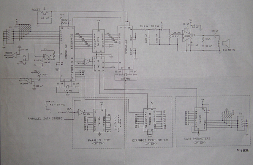
Schematic
Setting the Limits
The schematic used has three optional enhancements. The first is to allow parallel input of data. The second adds a RAM expansion for handling long strings of data. The third allows the CTS256A-AL2 chip to accept serial communications under different parameters. Each option has a valid need but I selected the RAM expansion and left the rest off.
What I Built
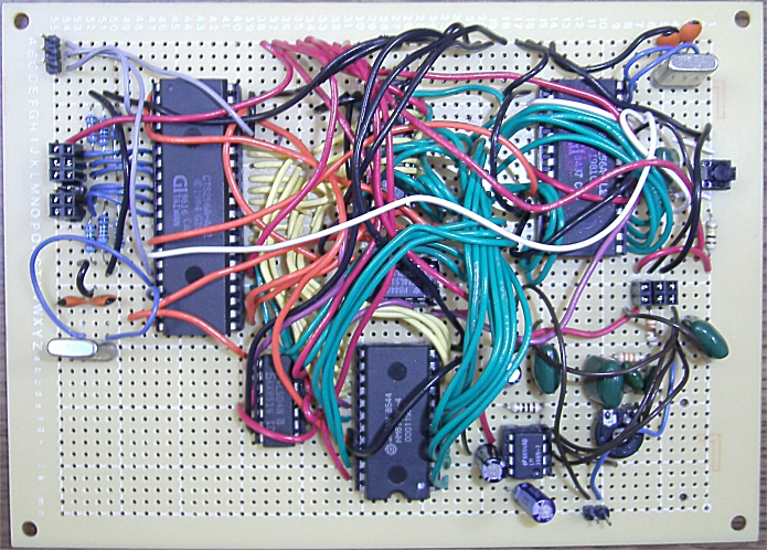
Aside from the crystal, the parts were obtainable via parts sties and eBay. I used a large prototyping and set about soldering the beast. I call it a beast because of the wire tangle I created. But don't take my word for it, look.
Layout
The board is layed out simply. The three header pins on the left are for serial communication (TX, RX, Busy). Below that are jumper switches to configure the serial interface and logic. The center top of the board has a two pin power connector (5V). The bottom right has a two pin connector for a speaker (8 ohms).
The center right has jumpers to isolate the audio amplifier. Why isolate? Well, I figured that I would build the amplifier last so as not to distract any testing needed on the rest of the circuit. But I actually built the amplifier on before any testing. I was going to complete everything before I tested anything.
Done but not Satisfied
At this point I tested the board and it worked. To be honest, the testing was hampered by not having an easy 7 bit, no parity, 2 stop bit communication rig handy. First I tried an arduino and played with the parameters. Then I used a terminal program and a FDTI cable on a USB port.
The testing made me wish that I added the parameter changing option on the schematic. But if I was going to do that, I might as well add the parallel data option. So, I did.
Expansion with All Three Options
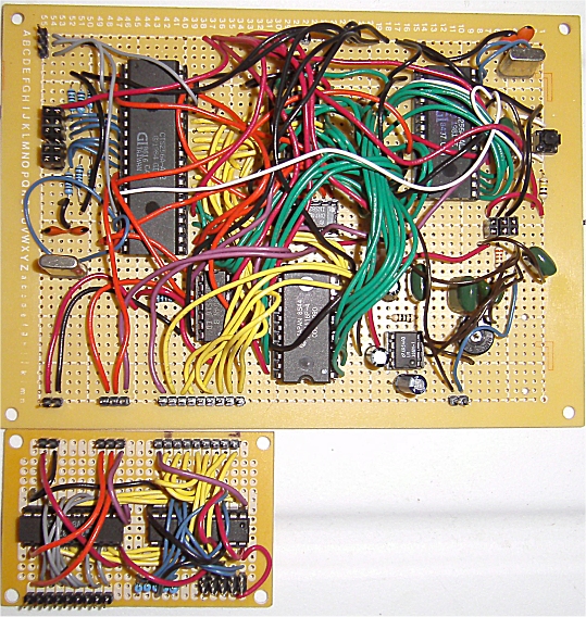
The beast now looks like this.
Because the board was too small for everthing to fit, I created a daughter board and interface pin layout. The first two pins are power. The next three pins are control lines for parallel data mode. The last set of pins is the serial parameter setting control line and data bus (yellow wires). Along the bottom of the daughter board are the prarllel data input pins and the serial parameter setting jumpers.
The only consolation to the rats nest of wires on top is the streamline underside.


